Combining Gates & Solving Problems
Introduction.
We have seen how logic circuits can be drawn as diagrams with inputs and outputs, and we can use truth tables to map out the range of possible results from these circuits.
However, we can also combine a series of logic gates to produce more complex circuits.
This allows us to solve problems and identify logical structures in how a computer works.
In this lesson, we’ll learn about:
- Combining logic gates to produce simple circuits.
- Applying logical diagrams & operators in truth tables to solve problems.


Producing Simple Circuits
We can start to put logic gates together to make larger circuits.
Each circuit can be represented as a Boolean expression, which will always start with an output, usually called Q.
To solve these, start with the brackets on the inside and work outwards.
Let’s work through three different expressions:
- Q = A AND (B AND C)
- Q = NOT (A OR B)
- Q = (A OR B) AND NOT C

Worked Example 1
Start with the brackets. This is the “B AND C” part.
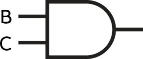
Add the outer expression; this is the “A AND” part.

Worked Example 2
Start with the brackets. This is the “A OR B” part.
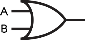
Add the outer expression. This is the “NOT” part.

Worked Example 3
Start with the brackets. This is the “A + B” part.
Add the outer expression. This is the “. C” part.

Solving Problems
We have seen how we can use Boolean algebra to represent some circuits.
We can build up truth tables to show all the inputs and all the possible outputs for any circuit.
We can then use this to work out which combination of inputs will give us a TRUE output.
The way to do this is to start small and build up your truth table column by column.
In your exam, you might need to complete a truth table for a given Boolean expression or draw the circuit diagram for a Boolean expression and then plot the truth table.
In order to solve this, you can follow some very simple steps:
- Build your inputs
- Check to see if any of your inputs have been NOTed
- Build your expressions from your initial inputs
- Look at the final output
Let’s now work through three example Boolean expressions.
Step 1: Build your inputs
We have two inputs, A and NOT B. So, we need 4 rows.
Step 2: Check to see if any of your inputs have been NOTed
Yes – B has been NOTed, so add a column for NOT B.
Notice how all we have done is flip the B column values.
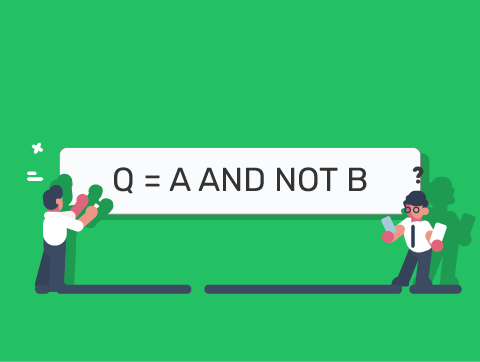
Step 3: Build your expressions from your initial inputs
Now, we need to add the expression by comparing the A column and the NOT B column.
As it is an AND gate, the output will be true if both inputs are true.
Step 4: Look at the final output
We can see that there is only one possible input to this circuit that gives a TRUE output.
When A = 1 and B = 0.
First, we have three inputs, so let’s see the truth table outline. We should have 8 rows this time.
They haven’t so we can skip this step.
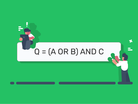
First, we have A OR B – ignore C for the moment.
Now, we can add the AND C part.
Remember it’s AND – so it’s where we have a 1 in the A OR B column, AND we have a 1 in the C column.
The following table shows the combinations of A, B, and C that give us a TRUE output.
First, we have 3 inputs, so let’s look at the truth table outline. We should have 8 rows.
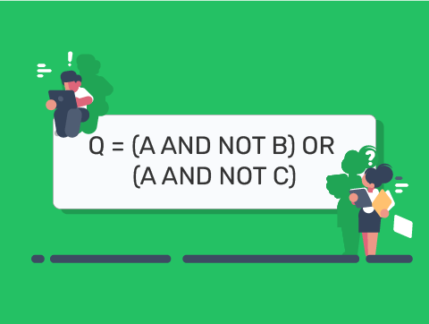
Yes – we have NOT B and NOT C, so we add these columns.
First, we have A AND NOT B, so we add this column – again, the output is TRUE when both inputs are TRUE, as it is an AND gate.
Now let’s add A AND NOT C.
Now we can build up our final expression where we have a 1 in the (A AND NOT B) column, OR we have a 1 in the (A AND NOT C) column.
So here we can see that there are only 3 possible inputs to this gate that give us an output of true:
Lesson Summary
You can combine logic gates to draw Boolean expressions.
Truth tables can be used to work out the outputs of any Boolean circuit.
They can be used to work out the Boolean algebra of any circuit.
The truth tables follow four rules:
- Step 1 – Build your inputs
- Step 2 – Check to see if any of your inputs have been NOTed
- Step 3 – Build your expressions from your initial inputs
- Step 4 – Look at the final output.

- Electronics
logic gates (practice problems)
Related documents
Add this document to collection(s)
You can add this document to your study collection(s)
Add this document to saved
You can add this document to your saved list
Suggest us how to improve StudyLib
(For complaints, use another form )
Input it if you want to receive answer
IIT JEE and NEET Physics @ Venkats Academy
Venkats Academy is a free Physics resource from a teacher with 20 plus years of experience and it is straight to the point from basics to advanced topics in detail for all IIT-JEE and NEET aspirants and high school students across the globe. It is now a combination of website and a Youtube Channel.
- JEE and NEET Physics @YouTube
- CLASS 11 Videos
- CLASS 12 Videos
- NEET CLASS 11 Questions
- NEET CLASS 12 Questions
Solving Problems on Logic Gates Concepts
.jpg)
No comments:
Post a comment.

More results...
- View all quizzes
- GCSE Concepts & Quizzes
- A Level Concepts & Quizzes
- Little Man Computer (LMC)
- Computer Networks
- Database Concepts
- Cryptography
- All Python Challenges
- Python Challenges – Beginner
- Python Challenges – Intermediate
- Python Challenges – Advanced
- HTML, CSS & JavaScript
- BBC micro:bit
- OCR J277/01 – 1.1 System Architecture
- OCR J277/01 – 1.2 Memory and Storage
- OCR J277/01 – 1.3 Computer networks
- OCR J277/01 – 1.4 Network security
- OCR J277/01 – 1.5 – Systems software
- OCR J277/01 – 1.6 – Ethical, legal, cultural and environmental impacts of digital technology
- OCR J277/02 – 2.1 – Algorithms
- OCR J277/02 – 2.2 – Programming fundamentals
- OCR J277/02 – 2.3 – Producing robust programs
- OCR J277/02 – 2.4 – Boolean logic
- OCR J277/02 – 2.5 – Programming languages and Integrated Development Environments
- OCR H446/01 – 1.1 The characteristics of contemporary processors, input, output and storage devices
- OCR H446/01 – 1.2 Software and software development
- OCR H446/01 – 1.3 Exchanging data
- OCR H446/01 – 1.4 Data types, data structures and algorithms
- OCR H446/01 – 1.5 Legal, moral, cultural and ethical issues
- OCR H446/02 – 2.1 Elements of computational thinking
- OCR H446/01 – 2.2 Problem solving and programming
- OCR H446/02 – 2.3 Algorithms
- 101 Extra Python Challenges
- 101 Python Challenges
- 101 Computing Challenges
- Become a member!
- Your Account
- Solved Challenges
- Membership FAQ
Logic Gates Circuits
This set of challenges is designed to be completed with a logic board such as the Logic & Arithmetic board designed by the University of Southampto n and the UK Electronic Skills Foundation .
Alternatively, if you do not have access to a physical kit, you can still complete these challenges using our online logic gates circuit simulator
Step 1: The Main Logic Gates

Step 2: Logic Gates Circuits

Step 3: Logic Problems

Create and test a logic gates circuit to control the internal light (X) of the car based on whether a door (J, K or L) is open (1) or closed (0).

- Input J: Whether the burglar alarm is activated (1) or not (0).
- Input K: A motion sensor can detect movement (1) or not (0).
- Input L: A door sensor can detect if the front door is open (1) or is closed (0).
The alarm siren (X) should be on if the alarm is activated and the motion sensor detects a movement or the door sensor detects that the door is open.
Create and test a logic gates circuit to control the siren of this burglar alarm based on the three inputs J,K and L.

- The phone is receiving an incoming call. (input J = 1)
- The phone sound is on. (input K = 1)
- The phone is not on airplane mode. (input L = 0)
Create and test a logic gates circuit to control whether the ringtone of a smartphone is on (X=1) or not (X=0) based on the three inputs J, K, L.
Extension Task: The Mystery Gate!

Did you like this challenge?
Click on a star to rate it!
Average rating 3.2 / 5. Vote count: 112
No votes so far! Be the first to rate this post.
As you found this challenge interesting...
Follow us on social media!

Other challenges you may enjoy...

Recent Posts
- Chess Challenge: Checkmate in one move
- 101 Computing Dashboard
- The Egg Farmer’s Puzzle
- Name the Country: Python Challenge
- Periodic Table of Elements – JSON Challenge
- Computer Software Card Game
- For Loops Challenges
- The Programming Skills Survey
- Parameter Passing: Take the Quiz
- MS-DOS Emulator
- View more recent posts...
- View all our challenges...
- Take a Quiz...
Our Latest Book

- Computing Concepts
- Python Challenges
- Privacy Policy
Combinational Logic Circuit Word Problems And Solutions
In the ever-changing world of technology, it's important to stay up to date on the latest trends and developments. One such area of focus is combinational logic circuits. This type of circuit solves word problems and offers a multitude of solutions to complex mathematical equations. By understanding how to create and use these circuits, electrical engineers can gain a better understanding of the complexities of electronic components and systems. Combinational logic circuits are used to perform mathematical operations by combining simple elements such as logic gates, flip-flops, and multiplexers. These elements produce a combination of set outputs based on the input conditions. Engineers can use these outputs to solve various types of problems, from basic arithmetic to complicated puzzles. In order to construct a combinational logic circuit that solves a problem, the engineer must first identify the problem’s input and output signals. He or she then constructs the circuit using logic gates and other components. One example of a combinational logic circuit problem is an equation that requires the calculation of two numbers from a given set of digits. The circuit works by using two multiplexers to select two of the digits from the set, depending upon the inputs that are provided. The circuit then calculates the sum of the two selected digits and produces the result as an output. This type of circuit is useful for solving equations that require multiple results from a single set of data. Engineers also use combinational logic circuits to solve more complex problems. For example, a circuit could be designed to determine the shortest path between two points in a given graph. Such a circuit uses a set of logic gates to process the given input data and evaluates all the possible combinations. Once a solution is found, the circuit provides the output that indicates the best route between the two points. Combinational logic circuits offer a wide variety of advantages, including reduced design time and improved performance. While they can be used to solve many types of problems, they can also be adapted and customized to fit specific applications. With these circuits, engineers can explore new and innovative ways to process and analyze data. With ever-evolving trends in technology, combinational logic circuits are likely to play an even bigger role in the future of electronics.

Digital Logic Sparkfun Learn

Multiple Choice Questions And Answers On Logic Gates Electronics Post

Boolean Algebra Worksheet Digital Circuits
Physics Tutorial Combination Circuits

Minimization Of Boolean Functions Gate Notes
Combinational Logic Circuits

Solved Itce 112 Digital Design And 250 Logic Chegg Com

Exam Questions Logic Gates Bits Of Bytes Co
Combinational Logic Circuit Problems And Solutions Pdf Technical Books

Combinational Logic Circuits Functions And Classification

How To Give Solution A Problem Using Logic Circuit Steemit

Solved Converting Logic Gates To Boolean Algebra Equations Chegg Com
Examples Of Solved Problems For Chapter 3 5 6 7 And 8

Boolean Algebra And Reduction Techniques

Combinational Logic An Overview Sciencedirect Topics

Solved Questions Set 2 Combinational Circuits Analysis And Chegg Com

The Basic Elements Of Digital Circuits Mosfet Gate And Logic
K Maps Karnaugh Solved Examples Gate Vidyalay
Reset password New user? Sign up
Existing user? Log in
- Number Theory
- Probability
- Everyday Math
- Classical Mechanics
- Electricity and Magnetism
- Computer Science
- Quantitative Finance
Take a guided, problem-solving based approach to learning Logic. These compilations provide unique perspectives and applications you won't find anywhere else.
What's inside
- Introduction
- Puzzles and Riddles
- Multi-Level Thinking
- The Rational Detective
- Syllogisms and Sets
- Logic Machines
- Arithmetic With Logic Gates
- Propositional Logic
- First-Order Logic
Community Wiki
Browse through thousands of Logic wikis written by our community of experts.
- Truth-Tellers and Liars
- Cryptogram - Problem Solving
- Solving Propositional Logic Word Problem
- Mind Reading with Math
- Information Compression
- K-level thinking
- Chess Puzzles
- Arithmetic Puzzles - Operator Search
- Arithmetic Puzzles - Fill in the Blanks
- Elimination Grids
- Grid Puzzles
- Combinatorial Games - Definition
- Combinatorial Games - Winning Positions
- Tic Tac Toe
- Sprague Grundy Theorem
- Chess Puzzles - Reduced Games
- Chess Puzzles - Opening Strategies
- Chess Puzzles - Rook Strategies
- Rook Polynomial
- Game Theory
- Nash Equilibrium
- Zero-Sum Games
- Prisoner's Dilemma
- Braess' Paradox
- Utility Functions
- Cognitive Bias
- Monty Hall Problem
- Birthday Problem
- Two-Envelope Paradox
- Simpson's Paradox
- Berkson's Paradox
- Newcomb's Paradox
- Benford's Law
- Mathematics of Voting
- Survivorship Bias
- Russell's Paradox
- Zeno's Paradox
- Gabriel's Horn
- Truth Tables
- Proof by Contradiction
- Mathematical Logic and Computability
- Mathematical Logic and Computability II (continuation)
- Propositional Logic Using Algebra
- Venn Diagram
- Predicate Logic
Problem Loading...
Note Loading...
Set Loading...
Problem Solving with Logic Gates
Due: 5 pm Tuesday 18 September 2018
Summary: In this lab you will use logic gates in a circuit to solve a logical puzzle. Instead of building logic gates using transistors, we will use TTL chips, which have several logic gates in a single chip.
Collaboration: You will work during lab in randomly assigned pairs. You must complete the work together in these groups, whether during or after the scheduled lab time.
Submitting: After completing each exercise, show your completed circuit to the instructor or a course mentor. If you are unable to complete the lab during class time, schedule a time during office hours to demonstrate your circuit.
The Problem
There is an old puzzle in which a farmer F F must transport a wolf W W , a goat G G , and a cabbage C C across a river. However, the farmer can only transport one of W W , G G , or C C across the river at a time, and if left together and unattended, the goat will eat the cabbage and the wolf will eat the goat. Let F = 0 F=0 indicate the presence of the farmer on the west bank of the river and F = 1 F=1 indicate presence on the east bank. Use similar definitions for W W , G G , and C C .
TTL chips look approximately like this. They are 14-pin "dual in-line packages" (DIPs), meaning that the chips are long and narrow with 7 pins on each side. Each chip has a small notch in one end for orientation. When the notch is pointed upward as in the diagram, the pins are numbered from 1 to 14 starting in the upper-left corner and proceeding counter-clockwise.

For purposes of your logic design, note we have the following TTL chips available in the lab:
- 1-input inverter (NOT) (6 gates per chip);
- 2-input AND, OR, NAND, NOR, XOR (4 gates per chip);
- 3-input AND (3 gates per chip).
I will provide a pinout diagram, showing what each pin on each chip is for. Please note that the pinout for different chip types (AND, OR, etc) is different.
Please note carefully, that you must connect each chip to power and to ground. It is important that you use the correct pins for this . Reversing power and ground will damage the chip. Make sure you connect to +5v and ground, not the adjustable +v or -v rows.
Seating chips in the board
Please refer to the protoboard diagram provided in the lab handout, to locate the "channel" between banks of pin connection points. To seat a chip in the protoboard, orient it such that its notch is facing upward as in the diagram, then place its two rows of pins such that they straddle one of the valleys in the board. This helps you attach power and ground to the correct pins, and ensures that none of the pins are connected together.
The chips may take some careful coaxing to seat them properly. I suggest placing one row of pins loosely into their holes in the board, and then using a fingernail to get the other row of pins lined up and started into their holes. Once all pins have been started correctly, you can press firmly, and the chip should snap into place. (Please be gentle until the pins are started well, or they will get bent, but then do press firmly to make sure the chip is fully inserted and that each pin makes a good connection with the board.)
Removing chips from the board
Be careful not to pull chips out of the board at an angle, which could bend or break the pins. Grab the chip at the top and bottom edges (where the chip crosses the channel on the protoboard). If you cannot remove the chip by hand, we can remove it carefully using a small screwdriver.
Working with Resistors
Now that we're working with TTL chips and the logic switches in the lower left corner of your protoboard, you can safely omit resistors from your circuits. Instead of turning the circuit on and off, logic switches make a connection from your wire to either +5v or ground. That eliminates the need for pull-down or pull-up resistors. The other use case for resistors in our previous lab was to limit the current through transistors and LEDs. As long as you use the logic indicators on the right side of the board instead of raw LEDs, you can omit these resistors as well.
Please double-check to make sure your logic indicator and logic switch sections are set to TTL mode. While you're double-checking your board configuration, make sure your TTL chips are powered from +5v and ground, not the adjustable +v or -v rows.
I expect that you will be able to complete this work during normal lab time. Please show your work to me or a mentor after each step in the lab work section below. If you are unable to finish all of the steps below during our scheduled lab, you may save your circuit on the board. Once you have completed the lab, schedule a time during my office hours where at least one member of your group can demonstrate your completed lab and show
- Derive a truth table defining a function which gives 1 if the farmer is in danger of losing the goat or the cabbage. You may assume that a trip across the river can be made instantaneously, so that if an item (or farmer) is not on one side of the river it must be on the other side.
- Use a Karnaugh map to generate a sum-of-products expression for this function. Then simplify the expression further with boolean algebra. Your final result should include only 8 variables, including repeated occurrences of the same variable.
- Draw a logic circuit diagram that implements your function from step 2. Label parts of the circuit that should be wired to the logic indicators on your protoboard to show when the farmer is in danger of losing either the goat or the cabbage.
- Using TTL chips, construct and test a circuit that implements your circuit diagram from step 3.
- Propose a solution to this puzzle starting with F F , W W , G G , and C C initially on the west bank and must be transported to the east bank. Use your circuit to check your solution.
- Check the part number on each chip carefully as you get it from the supply cabinet, and as you put it back . If you can not see the number well, hold it up to the sunlight. This is can be surprisingly helpful.
- Make a diagram of your physical circuit as you build it, recording where each gate in your logic circuit diagram is located on the protoboard.
- As you make each physical connection between logic gates, check the connection off in your logic circuit diagram.
- Either arrange your switches for F F , W W , G G , and C C in the same order as they are in your truth table, or be very careful to translate between the two correctly when testing your circuit.
Acknowledgements
Based on the fox, goose, and bag of beans puzzle .
Copyright © Marge Coahran, Janet Davis, Charlie Curtsinger, and Jerod Weinman

Lab 2 - Problem Solving with Logic Gates
In this lab you will use logic gates in a circuit to solve a logical puzzle. Instead of building logic gates using transistors, we will use TTL chips, which have several logic gates in a single chip.
This laboratory is divided between pencil-and-paper exercises, and a physical implementation. Since the implementation is likely to take a full class period, you should complete steps 1 through 3 before the laboratory session.
The Problem
There is an old puzzle in which a farmer F must transport a wolf W , a goat G , and a cabbage C across a river. However, the farmer can only transport one of W , G , or C across the river at a time, and if left together and unattended, the goat will eat the cabbage and the wolf will eat the goat. Let F=0 indicate the presence of the farmer on the west bank of the river and F=1 indicate presence on the east bank. Use similar definitions for W , G , and C .
- Derive a truth table defining a function which gives 1 if the farmer is in danger of losing the goat or the cabbage. You may assume that a trip across the river can be made instantaneously, so that if an item (or farmer) is not on one side of the river it must be on the other side.
- Use a Karnaugh map to generate a sum-of-products expression for this function. Then simplify the expression further with boolean algebra. Your final result should include only 8 variables, including repeated occurrences of the same variable.
- Draw a logic circuit diagram that implements your function from step 2. Label parts of the circuit that should be wired to the logic indicators on your protoboard to show when the farmer is in danger of losing either the goat or the cabbage.
- Using TTL chips, construct and test a circuit that implements your circuit diagram from step 3.
- If you have time , propose a solution to this puzzle starting with F , W , G , and C initially on the west bank and must be transported to the east bank. Use your circuit to check your solution.
- Check the part number on each chip carefully as you get it from the supply cabinet, and as you put it back . If you can not see the number well, hold it up to the sunlight. This is can be surprisingly helpful.
- Make a diagram of your physical circuit as you build it, recording where each gate in your logic circuit diagram is located on the protoboard.
- As you make each physical connection between logic gates, check the connection off in your logic circuit diagram.
- Either arrange your switches for F , W , G , and C in the same order as they are in your truth table, or be very careful to translate between the two correctly when testing your circuit.
TTL chips look approximately like this. They are 14-pin “dual in-line packages” (DIPs), meaning that the chips are long and narrow with 7 pins on each side. Each chip has a small notch in one end for orientation. When the notch is pointed upward as in the diagram, the pins are numbered from 1 to 14 starting in the upper-left corner and proceeding counter-clockwise.

For purposes of your logic design, note we have the following TTL chips available in the lab:
- 1-input inverter (NOT) (6 gates per chip);
- 2-input AND, OR, NAND, NOR, XOR (4 gates per chip);
- 3-input AND (3 gates per chip).
I will provide a pinout diagram, showing what each pin on each chip is for. Please note that the pinout for different chip types (AND, OR, etc) is different.
Please note carefully, that you must connect each chip to power and to ground. It is important that you use the correct pins for this . Reversing power and ground will damage the chip.
Seating chips in the board
Please refer to the protoboard diagram provided in the lab handout, to locate the “channel” between banks of pin connection points. To seat a chip in the protoboard, orient it such that its notch is facing upward as in the diagram, then place its two rows of pins such that they straddle one of the valleys in the board. This helps you attach power and ground to the correct pins, and ensures that none of the pins are connected together.
The chips may take some careful coaxing to seat them properly. I suggest placing one row of pins loosely into their holes in the board, and then using a fingernail to get the other row of pins lined up and started into their holes. Once all pins have been started correctly, you can press firmly, and the chip should snap into place. (Please be gentle until the pins are started well, or they will get bent, but then do press firmly to make sure the chip is fully inserted and that each pin makes a good connection with the board.)
Removing chips from the board
Be careful not to pull chips out of the board at an angle, which could bend or break the pins. Grab the chip at the top and bottom edges (where the chip crosses the channel on the protoboard). If you cannot remove the chip by hand, we can remove it carefully using a small screwdriver.
Pull-down resistors
Recall that these are the resistors you need in your circuit to connect each switch to ground. In the previous lab, and in class notes, we used 15K resistors for this purpose. For this lab, you should use 150 Ohm resistors instead.
Informally, this is because the input pins on a TTL chip are made to “float” to a voltage mid-range between low and high. We can override that with a pull-down resistor connected to ground, but to do so we need to use a resistance that is smaller than that used internally in the chip.
Logic probe
Be sure the logic probe section of your protoboard is set to TTL, not CMOS logic.
Acknowledgements
Based on the fox, goose, and bag of beans puzzle .
Content for this course and the course website is derived from Janet Davis' offering of CSC 211 in fall 2013, and developed in collaboration with Jerod Weinman.
This website was built using Jekyll , Twitter Bootstrap , and the Bootswatch Cosmo Theme .

IMAGES
COMMENTS
May 16, 2023 · You can combine as many logic gates as necessary using the standard logic gates (NOT, AND, OR, XOR, etc.) ... 2.2 Problem solving and programming; OCR H446/02 – 2.3 ...
However, we can also combine a series of logic gates to produce more complex circuits. This allows us to solve problems and identify logical structures in how a computer works. In this lesson, we’ll learn about: Combining logic gates to produce simple circuits. Applying logical diagrams & operators in truth tables to solve problems.
LOGIC GATES (PRACTICE PROBLEMS) Key points and summary – First set of problems from Q. Nos. 1 to 9 are based on the logic gates like AND, OR, NOT, NAND & NOR etc. First four problems are basic in nature. Problems 3 & 4 are based on word statement. Problems 5 to 9 are on Universal gates.
In any electronic circuit we can execute a certain logic with the help of the logic Gates. Here we shall understand how to solve problems using this kind of logic and the digital algebra. There are different types of logic Gates as you mentioned in the previous post like OR gate, AND gate, NOT gate, NAND gate and NOR gate.
Problem: We introduced standard cell technology in section 3.7. In this technology, circuits are built by interconnecting building-block cells that implement simple functions, like basic logic gates. A commonly used type of standard cell are the and-or-invert (AOI) cells, which can be efficiently built as CMOS complex gates.
Mar 14, 2022 · Step 2: Logic Gates Circuits. By combining multiple logic gates together you can create a circuit that will “behave” a certain way. To record how the circuit “behaves” for any given set of inputs we use a Truth Table. For instance you can complete the Truth table for the following circuit:
Jan 24, 2020 · Engineers can use these outputs to solve various types of problems, from basic arithmetic to complicated puzzles. In order to construct a combinational logic circuit that solves a problem, the engineer must first identify the problem’s input and output signals. He or she then constructs the circuit using logic gates and other components.
Take a guided, problem-solving based approach to learning Logic. ... Arithmetic With Logic Gates; Propositional Logic; First-Order Logic; Community Wiki.
Sep 18, 2018 · Summary: In this lab you will use logic gates in a circuit to solve a logical puzzle. Instead of building logic gates using transistors, we will use TTL chips, which have several logic gates in a single chip. Collaboration: You will work during lab in randomly assigned pairs. You must complete the work together in these groups, whether during ...
Lab 2 - Problem Solving with Logic Gates. In this lab you will use logic gates in a circuit to solve a logical puzzle. Instead of building logic gates using transistors, we will use TTL chips, which have several logic gates in a single chip. This laboratory is divided between pencil-and-paper exercises, and a physical implementation.